In
a previous article I discussed the MOS 7600 and 7601 "Pong in a chip" ICs, manufactured by MOS Technology (of the famous 6502) and actually used in a number of late 1970s Pong clones, including two that eventual parent company Commodore Business Machines
sold under their own name. Most notably they appeared in the Coleco Telstar Arcade console, an unusual "triangular" machine in which specific variants of the 7600 were used as its cartridges, but were also used in a number of other Pong clones through around 1978.
The question at the time was whether the 7600 actually had ROM in it (i.e., was a true microcontroller running a stored program), or whether it was simply playing games using discrete circuitry. The Telstar Arcade — and its relative, the confusingly named Telstar Gemini, not to be confused with the separate Coleco Gemini — demonstrated that other variants of the 7600 were capable of more sophisticated games than just ball-and-bat Pong variations, including primitive versions of pinball and road racing, even though most systems using the 7600 used it purely for Pong. On the other hand, no data sheets have survived to the present day and at the time my Google-fu uncovered no die photos to review, so I could find no substantiation for the occasional claims that it did.
Well, we now definitively know the answer and a bit more thanks to Sean Riddle, who actually did decap and photograph a 7600-002 die (the variant in Telstar cartridge #1, with racing, Pong and skeet shooting) and a 7600-001 (the most common three-Pong-and-skeet variant used in many machines, as well as in Telstar cartridge #2), and to Ken Shirriff, who made an extensive survey of the die, discussed with Sean and I attributes he noted, and posted a thread about it. Here's my own summary of the discussion plus a few other details I've run across since writing the original post.
First, let's not bury the lede; there is mask ROM on the 7600/1. In fact, it's a surprisingly sophisticated microcontroller for the time. Here is Sean's original 7600-002 die photo with Ken's notes (most of these images were marked up by Ken), reproduced with their gracious permission. This image is based on his notes though I made this higher resolution image in Krita.

And here it is with its own board markings enlarged. For review, the 7600-002 variant plays three very different games: racing, not seen on any other variant; skeet; and one pong ("tennis") game. The -002, -003 (naval battle, speed ball [Pong with a central block for bounce shots] and a two-player skeet) and -004 ("paddle" pinball and skeet) only were used in the Coleco Telstar cartridges (along with -001) and the Coleco Telstar Gemini (no cartridges, plays only -004). The 7600-001, along with its PAL variants 7601-001 and 5601, were used everywhere else including the Commodore TV Game series. Superimposed on the same image we show enlargements of the on-die MOS logo with some unknown production markings, plus 7600 ("7600C") and 002 ("002E") markings.

The 7600-001 is similar, except it has different production markings (the numbers 1-5 but no letters beneath the MOS logo, plus 7600C and 001F). If we compare Sean's two dies, i.e., the 7600-002 against the 7600-001, most of the major changes are in the shape programmable logic arrays (PLAs) and program ROM, as you would expect for a cartridge with different graphics and games:

The chip itself is PMOS, or P-channel metal–oxide–semiconductor, the technology predating more recent NMOS and CMOS chips. However, NMOS already existed when the 7600 was being designed (the original 6501 and 6502 are themselves NMOS, and slightly predate the 7600), so the use of PMOS was likely a cost-cutting move consistent with MOS Technology getting a design to market quickly for cash during the Motorola lawsuit. Further credence for this chip being cheap comes from another of Ken's observations, that the chip has depletion-mode pullups (i.e., the gate of the pull-up transistor is connected to the output, not to +V), but uses metal gates. Metal gates are nowadays commonplace in modern chips, but for about three decades (1977 or so through around 2007) up to the 45nm node, polysilicon was more common for expedient fabrication. Using metal gates by this point in time (circa 1976) would have been old-fashioned but also less expensive. As a result the chip extensively uses PLAs — big networks of NOR gates with fixed interconnects mapping inputs to outputs — to sequence its operations, since metal gates of the time were less efficient for routing and PLAs would facilitate greater density. Ken estimates the chip has around 16,000 transistors, about double that of the Zilog Z80, and over four times that of MOS's own 6502.

The chip uses 13-bit words in its stored program, embodied in 512 words of mask ROM at the lower left, and the "CPU" that interprets them roughly surrounding it. The chip is almost entirely based on shift registers, i.e., cascaded flip-flops such that the output of one is connected to the output of the next and signals serially propagate bit-by-bit clock tick by clock tick. This is obviously slower but compared to RAM or flip-flop registers shift registers also require fewer transistors, demonstrating another cost-conscious aspect of this design. A small vertical block to the upper left of the mask ROM and a small horizontal block to the upper right of the mask ROM (both in red) compose an eight-bit shift register; the left block has 6 bits to choose one of the 64 columns, and the right block has the other two bits. Because the left side grounds alternating rows, the first shifted bit selects even or odd rows, and the right two bits choose one of the resulting four 13-bit words in that column. Together these appear to form the program counter.

The value of the program counter cycles serially through the ROM's decoding logic, located immediately to the right of the ROM, and into the area in green which serves as the incrementer. This is a half-adder with a buffer for carry. From there it passes to the area in blue, a small PLA which generates the next address. It is possible, and even likely, that consecutive instructions are not stored at numerically adjacent "addresses"; moreover, the actual bit patterns for individual instructions could be in one of around eight possible arrangements and the exact instruction encoding is not obvious. The 13 bits of the current instruction pass through the instruction decoder to set control signals that exit from the decoder to be routed elsewhere. The area in purple drives the two-phase clock signals used by the shift registers.

If we zoom in on the area immediately above the ROM's address decoder (the "stairstep" binary pattern), there is another set of three shift registers, each 9-bit. To orient you, the address PLA in blue from the previous picture is at the bottom right in this one. The shift registers form a three-level subroutine return stack, which is unexpectedly complex for a chip of this sort. The address PLA supports at least six types of branching instructions, including a hard reset (clear stack and PC to 0), step to next instruction, jump, call, return, and interrupt (i.e., a call to a fixed address). These instructions plus conditional forms are selected from by at least three bits in each opcode. Call and interrupt instructions push the current program counter plus one onto the stack, which is nine-bit to capture the even-odd select bit, and return instructions pop it off.
There is no RAM or a discrete register file on the chip (as such) either; all storage is in shift registers too. Although they appear in other places, the biggest conglomeration is in the area marked "shift registers" where there are 72 bits available. There is probably some working storage here, and some variable storage such as scoring, but this region is also used to control graphical elements (I'll discuss presently). Although the program may be able to read the console switches and some other values directly, the firmware primarily relies on signals when a collision or detection is registered. For example, the gun circuit registers a hit when the player pulls the trigger and the skeet sprite is visible to the photodetector in the pistol (and thus relies on a CRT television's scanning beam to function), and the program increments the score accordingly.

The graphic display is more complicated and less well understood. Counting pixels in the racing game, the display appears to be roughly 88x118, though some of that is overscan, and movable screen elements can apparently use half-height rectangular pixels (this is most obvious in the racing game here). The use of slow bit-serial shift registers for game state would make program-controlled drawing fairly difficult, and there are only 512 instructions anyway to be split among up to four games per chip, so it's very unlikely that the stored program code does any graphics programming other than to control the position and activity of on-screen elements. For example, the scores are probably stored somewhere in the 72-bit shift register area and the stored code manipulates it directly according to its programming, but this also propagates to the graphics circuitry to draw the on-screen score digits from the same value without requiring a separate action from the processor. We saw an example of this in the scoring for the racing and pinball games, where the +100 that appears when we roll the score appears to be a separate bit. When that bit is set, then the graphics circuitry automatically draws a 1 in the proper place. The stored program can also set and change bits here to turn off hardware display elements not used by the current game.

Instead, the shape data is fixed, and most likely encoded in the region marked "shape PLA." Unfortunately, there is no way to see a bit pattern that corresponds to a ball, paddle, digit or sprite because one PLA column can match multiple bits and the bit order is necessarily scrambled. Additionally, the horizontal drive lines are split, meaning that even though the red and blue regions are structurally part of one PLA, they seem to receive separate inputs. However, the current theory is that the red regions cause a particular object or pattern to be drawn at the location specified by the shift register to the right of them, encoded in the right half of the blue area, plus other pertinent inputs such as the current game in play. The left half of the blue region is an eight-stage ring counter that represents the current coordinate within the object being drawn. This particular structure appears to be repeated at least twice.

The way the paddles in particular are drawn is especially ingenious; in fact, the firmware doesn't even need to position them. The paddle controls are simple potentiometers feeding into an R-C circuit (external to the chip, not shown here) that discharges at a rate based on the pot's resistance. This then feeds into an on-chip comparator in the region marked "paddles," delaying drawing the paddle a number of scanlines based on the pot's position until the comparator triggers, thus eliminating the need for a more complex solution like an A-D converter (cheap!) and automatically drawing the paddle at the proper location without any intervention from the firmware. You'll notice a large number of shift registers in the paddle region as well, which serve as a delay line: when the comparator fires, a control signal goes to the shape PLA to start drawing, and (at least for the -002) a 16-bit shift register holds the signal for 16 scanlines, the height of the paddle. The -004 has complex multicolumn paddles of different heights, though the shape PLA would still handle the individual columns. The blue region is one paddle's control and there is one for each paddle. In non-Pong games, presumably a bit is set in the "shift registers" workspace and the paddles are not drawn.
A smaller PLA can be seen near the bottom of the image. This controls how the ball is reflected back. In the original Atari Pong, it didn't matter at what angle the ball hit your paddle; it mattered at what point it hit it. If it struck in the centre, it was returned straight back, with correspondingly more acute angles of return towards the edges of the paddle. Atari Pong had seven zones, but the 7600 implemented just five as documented in the manual for the Commodore TV Game 3000H. If you look at the differences between the first four rows of the PLA (rotate it 90 degrees vertically in your mind's eye if this doesn't make sense), you can see the five zones, the two peripheral zones being mirror images of the other with a single central zone.

The video PLA above the shape PLA takes in the pixels as they clock out and maps its vertical inputs into ten horizontal outputs (though Ken points out that the top and bottom of the video PLA are frequently the same, meaning there are often two groups of five outputs which are identical). This appears to specify a specific game-dependent colour value.

From there the video PLA signals enter the upper left corner of the die and are processed. There are multiple small PLAs here which take the 10 signals or two groups of five and turn them into six video signals which exit through the top six pins. These signals are generated through the six blue driver circuits which are necessary to generate sufficient current flow with metal-gate transistors. In this arrangement the smaller transistors feed into larger ones which feed into still larger ones until the necessary amount of current is reached. These video signals are (at least) pixel video and horizontal and vertical sync, along with some sort of colour value encoding. Pin 24, second from the left, has a 15.734kHz signal consistent with the NTSC horizontal scan rate. But how do we get actual NTSC (or PAL, for the 5601 and 7601) colours the TV can display? Well, that looks like it's actually
external to the chip.
Let's compare a couple systems. One of the consoles we explored in the last article was the Radofin SC Eight Thousand (or SC8000 for short), an el-cheapo-Pongo system that was sold at Kmart stores in the United States. It has a display like this:
The 7600-001 in the SC8000 plays the standard three Pong variations, plus a skeet shooting mode. The background colour changes per game, including to black for the skeet mode (or else the photodetector would trigger everywhere). Here, in "tennis" mode, the game displays cyan text over a blue background with green and orange bats. The 7600 chip in this system is dated 31st week 1977.
Sean was able to get another MOS 7600-001 system, the 1977 Venture Electronics Video Sports VS-7. Sean's picture of the chip also shows 31st week 1977 (picture courtesy him).
If the actual colour values were being generated on-chip, then these systems should have identical graphics because the chips are identical. But they don't. The same game on the VS-7 has an orange background, and everything else is white:
(These screen grabs came from
this YouTube video. Thanks, Joe's Classic Video Games!) In fact,
all of the games — except skeet, as expected — on the VS-7 are orange, despite multiple colours on the SC8000. For that matter, there's also footage of the Coleco Telstar Arcade cartridge #2 (which I don't currently have), which also has a 7600-001, and it too has
a different colour palette despite exhibiting all the other quirks of the NTSC 7600-001 like oversized score numbers. (The score numbers on the 5601, 7601 and all other 7600 variants are smaller.)
The six pins exiting the chip at the top go through a couple components before they reach the RF modulator and then the television. To get a closer look at this, I managed to find an apparently busted SC8000 for cheap that I planned to disassemble. Amusingly, the darn thing (despite obvious abuse) actually still works and plays fine. However, it has a 7600-001 that is over six months older than the one in Sean's VS-7 and my "nice" SC8000, with a date code of 2nd week 1977. (Parenthetical note: the R-C circuits for the paddles are below the 7600 and the rotary game select switch.)
Compare with the very first NTSC 7600-001 system, the Allied Leisure Name of the Game
[update: we have one!],
model A-100, with the earliest 7600 I've seen yet from 47th week 1976 as proof that the chip existed that far back. [Actually, our local NotG, the less common 2-player model A-300, is even older and
in ceramic, from the 42nd week 1976. I have yet to find a chip older than that.]
This older SC8000 also plays identically to the later unit and with the same colour palette. Both the VS-7 and both of my SC8Ks are flanked by two small ICs, a quad bilateral switch (a CD4066AE in the SC8K, a CD4016 in the VS-7) and a hex buffer-inverter (CD4009AE vs CD4049). Similar circuitry is inside the Telstar Arcade, with different palettes for each cartridge. NTSC colours are produced by phase-shifting the 3.58MHz colour subcarrier frequency, generated by the crystal above the 7600 next to the can capacitor. Based on incoming colour encoding data from the chip, the hex inverter generates the phase shifts and the quad switch selects the desired phase, ergo the colour. The inputs for the hex inverter are likely controlled by the rotary game select switch and constitute the palette in use, but the VS-7 appears to have only two sets of palette circuits (orange/white and black/white) while the SC8000 has four. This colourized output then feeds the RF modulator (to the right) and exits to the TV through the wire at the bottom right.
Speaking of, how are clocks generated on the 7600/1? They also come from the same 3.58MHz colourburst crystal:

The two pins Ken marked OSC go to and from the crystal. The yellow box drives the crystal's waveform from the top pin to the bottom one, with a capacitor about two-thirds of the way down. The red box above it is an operational amplifier ("op amp") that turns the nice sinusoidal voltage from the crystal into square wave pulses based on a reference level set by nearby resistors. The green box has a pair of latches to clean up this signal, which then feeds into the blue box, a linear-feedback (you guessed it) shift register used as a clock divider. This doesn't really tell us what the actual clock speed of the chip is, though, and some cheating must be going on because the 15.7kHz horizontal signal we know the chip generates for video is not an integral divider of the 3.58MHz colourburst (the scan rate may vary, or some other circuitry could be involved); we only know that the chip's internal clock can be no faster than that.
That leaves sound. All Most 7600/1 systems have internal speakers and do not send audio to the TV [turns out there are exceptions], which makes it easy to test them: power them on, press some buttons and see if they make noise.
The blue region accepts control lines from the instruction decoder, meaning the stored program can trigger tones directly, though there may be other ways to do so. At least three small PLAs exist as sound sources of varying frequency (there is only one voice that I can determine), with four volume levels (off, one-third volume, one-half volume and full volume). Audio then passes to the three large driver transistors in the red region and out through pin 13 to the speaker.
We compared the 7600 to the "Gimini Economy" (General Instrument 8600) games-in-chips in our last article as well, and Sean has also decapped several of these. Unlike the 7600/1, and as I had suspected, these are not microcontrollers — everything is indeed hardwired. Cole Johnson has an excellent explanation and even simulations of the AY-3-8606 breakout and AY-3-8605 sub shooter games (as well as the earlier and less sophisticated AY-3-8500 Pong-in-a-chip). There are no ROMs on these and they consequently have substantially fewer transistors, just a couple thousand (2975, 2777 and 2318 respectively, even fewer than the 6502, and far fewer than the monstrosity here of interest). For as cheap as the 7600 must have been, I would imagine these would have been even cheaper.
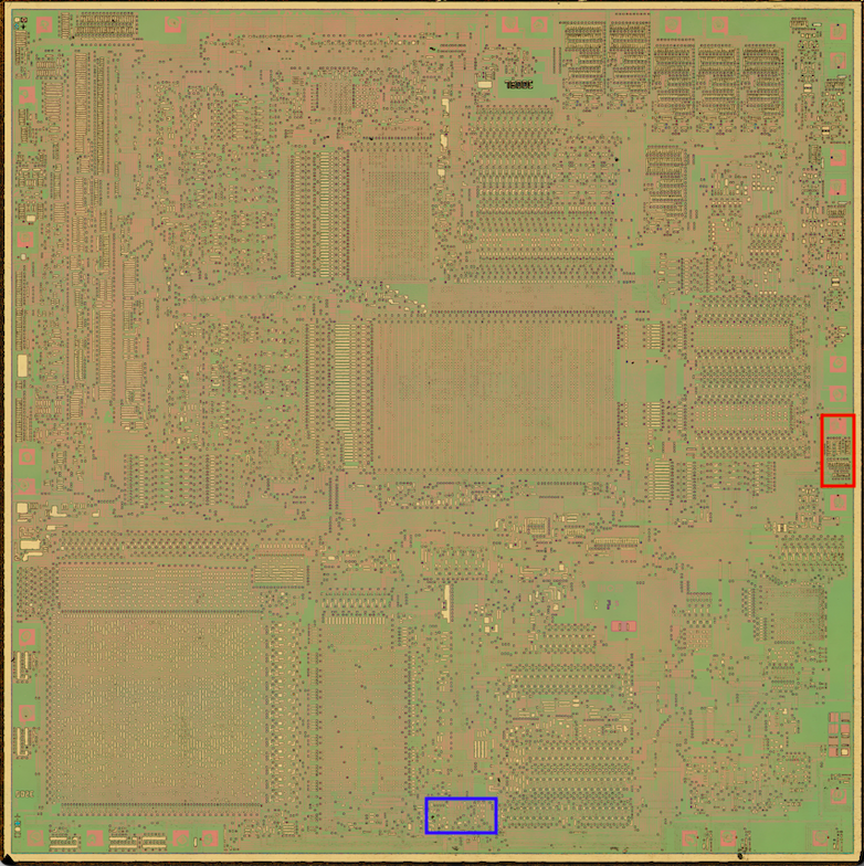
As a post-script, the 7600/1 was not MOS's only game-specific chip, though it was the only game chip Commodore Business Machines, their parent company from 1976 on, was known to have used in its own products. Sean also found and decapped the MOS 7651, so far only identified in the Grandstand Pocket Match of the Day soccer game in the UK.
The large mask ROM is obvious, but also what looks like a discrete true register file instead of the scattered shift registers in the 7600 (see Ken's discussion of the
Zilog Z80) or the far more parsimonious all-over circuitry of the 6502's registers. Whatever MOS's game chip history may have been, they made some truly whopping designs even if they didn't end up lasting very long in that market.
Again, many thanks to Ken Shirriff and Sean Riddle for their help in solving this mystery!


No comments:
Post a Comment
Comments are subject to moderation. Be nice.